English
 Polski


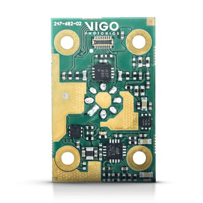
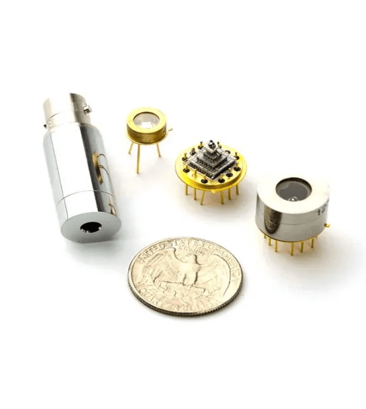
New InAs and InAsSb IR detectors
Watch our latest webinar

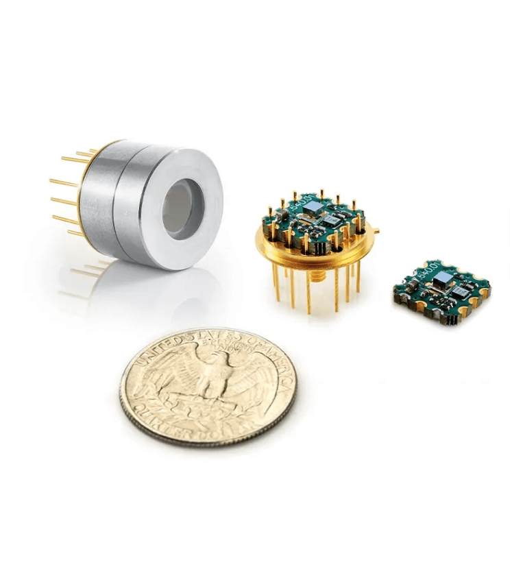
A small and affordable solution for gas sensing
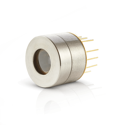
InAs/InAsSb SL Technology
Infrared detectors for space application


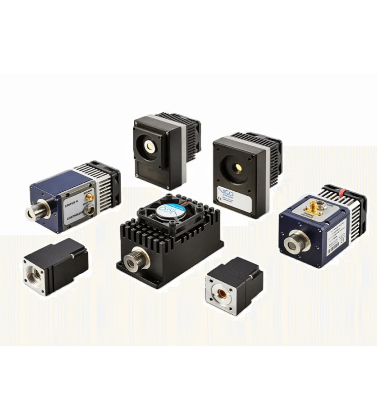
Our main products
Key applications of VIGO Photonics detectors


Key applications of VIGO Photonics detectors
Industrial IR Sensor
The detectors are used for monitoring process gases in chemical, refining, power generation, food and aerosol production industries.
Automotive sensor
The unbeatable speed and sensitivity of VIGO Photonics detectors make them useful in applications where the response time is a matter of safety of hundreds of people.
Laser Gas Leak Detection with Infrared
VIGO Photonics has developed a unique technology of manufacturing instruments for a quick and convenient detection of a 1 – 16 μm infrared radiation.
Infrared Detectors for Security and Defense Applications
The device will be designed to search places where an explosion, a gas or terrorist attack may occur. Next, the detection system will notify about possible risks or threats
Plastic Sorting Using Mid IR Linear Detector Array
Development of effective methods for the mass production of plastic objects has revolutionized many industries, but what about mass recycling methods?

VIGO Photonics
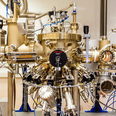
VIGO Photonics S.A. is a world-leading manufacturer of uncooled infrared photon detectors. In the 1980’s, a team led by Professor Józef Piotrowski, Ph.D., developed at the Military University of Technology in Warsaw, Poland a special technique for manufacturing detectors operating without cryocooling, which was subsequently implemented at the Company.
Our company


What’s new in VIGO?