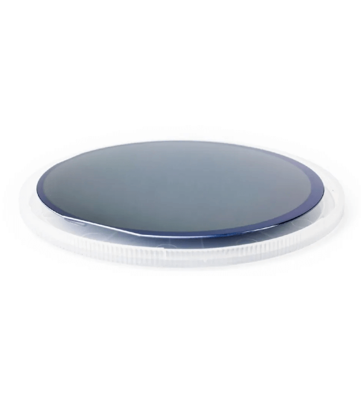
The so-called InGaAs material refers to a complete epitaxial stack composed of a variety of layers, with InGaAs forming the key part – the absorption – and being responsible for the material’s optical properties. The InGaAs layer itself is a III-V semiconductor that belongs to the family of In(x)Ga(1-x)As(y)P(1-y). For binary GaAs, InP, GaP, or InAs, the x and y are set to 0 or 1. In quaternary InGaAsP and ternary InGaAs a variety of x and y values are possible, and each combination will tune the semiconductor to different applications.
Adjusting the proportion of Indium to Gallium and Arsenic to Phosphorus affects the energy band-gap and lattice parameter of the compound. By the rule, as given by Planck equation E=hν, the higher the energy the higher the frequency, which is inversely proportional to the wavelength. An adjustment of x in In(x)Ga(1-x)As allows to lower the energy band gap and therefore make the light spectral range longer, but this happens at the cost of changing the lattice constant and mismatching to an InP substrate. The lattice constant is a key value to designing the epitaxial stack and predicting the strain that can occur in the layers.

Cutt-off wavelength
The quaternary InGaAsP, which would be the result of mixing all four chemical elements, finds its usage in the 1.0-1.6um range, as relevant band-gaps will be achieved when lattice-matching InGaAsP to InP. Omitting the Phosphorus (y=1), to create the ternary InGaAs, would allow to lattice-match to InP at the composition of Indium at 53% – In(0.53)Ga(0.47)As – with energy band gap of 0.73eV equal to cut-off wavelength of around 1.7um.
Cut-off wavelength means that only wavelengths shorter than the given value will be absorbed and any values above will have very low or none detectivity; a parameter measured as D* (cm Hz^1/2W^-1) and describing a normalized signal-to-noise ratio of a device.
Standard InGaAs vs. Extended InGaAs
InGaAs materials with InGaAs in the absorption layer and cut-off wavelength set at 1.7um (lattice-matched to InP) are often referred to as Standard, while materials with cut-off above 1.7um (lattice-mismatched) are called Extended.
The reason to extend the detection range to higher values, such as to 2.6um, is simple and answers the need of an application, but the execution imposes a great challenge. A lattice-mismatch requires a specially designed and graded buffer layer, which will act as a bridge between the substrate and the absorber. This solution is, however, never ideal, and a number of misfit defects and anomalies in dark current can occur. As such, once developed, the buffer layer is often considered the company’s secret.
Epitaxial stack design
Material performance

VIGO’s InGaAs results
In the characterization process of our InGaAs materials we start with an X-ray diffraction. The correct placement of the InGaAs peak, as shown on the right, confirms that the material of the absorption layer has precisely tuned chemical composition with the lattice parameter equal to the one of the InP substrate. Any shift of the peak would indicate a non-consistent composition of that layer and potential generation of misfit dislocations.

XRD scan of In0.53Ga0.47As lattice matched to InP
For InGaAs Extended material, the lattice mismatch between the absorber and the substrate is desired. We use X-ray to calculate the peak location shift to verify the absorber’s chemical composition and correct tuning to a specific wavelength. The lack of a clear InP peak in this case is the result of grading growth applied directly on the substrate, which is required to handle the strain between layers of different lattice parameters.

XRD scan of extended In0.818GaAs. Da/a= +19750 ppm